
When repairing military and civilian electronic products, do you often face the frustrating problems of missing schematic diagrams, time-consuming troubleshooting, and low efficiency? Don't worry. Today we introduce a highly practical board-level defect detection method — flying probe test-based detection technology.
This technology uses 3D-Xray for computed tomography, extracts flying probe coordinate information, and thereby achieves defect detection on PCBA board level. For boards with missing schematic diagrams, flying probe testing is extremely "flexible": it requires no fixtures or dedicated test points and can directly test by probing component pads.
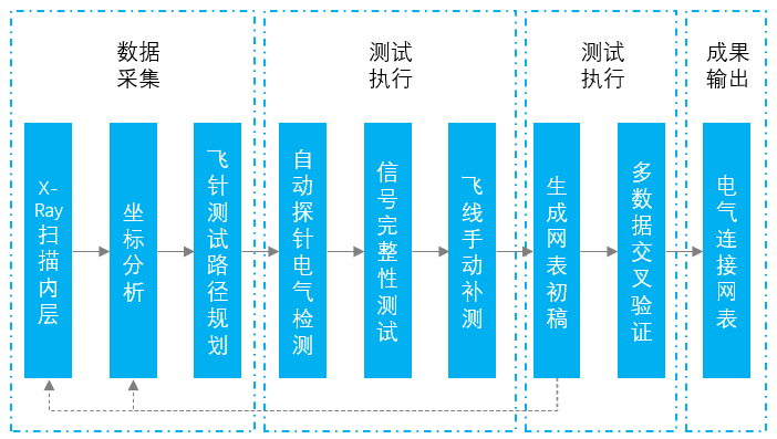
Flying Probe Test Preparation: Manually define test points and establish "temporary networks".
In the absence of Gerber files, the core of flying probe testing lies in manually screening test points and reversely establishing circuit connection relationships, with the specific steps as follows:
a.Screen Test Points
Visually identify "key measurable nodes" on the PCB.
b.Reverse Establishment of Network Topology
A network refers to a "set of interconnected test points" (e.g., power supply networks, signal networks). Without original diagrams, it needs to be manually mapped through the "continuity scanning" function of flying probe testing.
02.Flying Probe Test Fault Localization: Identify Anomalies by Combining Function and Experience
Based on manually established test points and temporary networks, flying probe testing can detect the following faults, which can then be judged as "true faults" by combining with experience.

a. Short-Circuit Faults
If the test detects that the "power supply network is connected to the ground network" (i.e., the resistance is close to 0Ω) or that "two independent signal networks are unexpectedly connected", it can be determined as a short circuit.
Localization Method: Gradually narrow down the scope through flying probe testing. For example, in case of a power supply network short circuit, disconnect components in the suspected faulty area (such as removing power supply chips and capacitors), and re-test the continuity between the power supply and ground until the short-circuit point is found (e.g., capacitor breakdown, internal PCB wire adhesion, etc.).
b. Open-Circuit Faults
If a functional module (e.g., a USB interface) has no response, and it is inferred from the temporary network that its pins should be connected to the pins of a certain chip, but the flying probe test shows that the resistance between the two is greater than 100Ω, it can be determined as an open circuit.
Localization Method: Along the inferred connection path (e.g., from the chip pins to the interface pins), observe the direction of the PCB surface wires, and use flying probe testing to check the continuity of vias and pads on the path to find the break point (e.g., wire breakage, via blockage, etc.).
c. Component Anomalies (Without a BOM, it is necessary to infer whether components are defective by combining flying probe test component parameters with visual identification)
i. Resistors: Test the resistance value. If it is much higher than the color ring marking or infinite, the resistor may be open-circuited; if it is much lower than the marking, the resistor may be burned out.
ii. Capacitors: Test the capacitance value (supported by some flying probe equipment). If the capacitance is 0 or far exceeds the nominal value, the capacitor may be defective. Test the insulation resistance to ground; if it is close to 0Ω, the capacitor may be short-circuited.
iii. Chips: Internal functions cannot be directly tested, but pin continuity can be tested. If the chip's power pin is disconnected from the power supply network (i.e., open circuit) or the ground pin is disconnected from the ground network, there may be a soldering problem. If the power supply is directly connected to the ground (i.e., short circuit), the chip may be internally broken down.
03.Component Identification and Replacement: Reverse Deduction of Models and Parameters
Without a BOM, the core of component replacement is "visual identification + parameter measurement + functional matching".
04.Board-Level Functional Testing
| Test Item | Test Content and Purpose | |
| Power-On Safety Test of the Board Under Test (Insulation and Short-Circuit Test of Power Supply Ports) | Detect whether the insulation resistance of the power supply ports meets the standard and whether there is a short circuit; avoid equipment damage and safety accidents; ensure initial power-on safety | |
| Power-On Voltage, Current and Power Test | Monitor the voltage, current and power at the moment of power-on and during stable operation; judge whether the power supply is normal; evaluate the rationality of power consumption; identify anomalies such as overvoltage and overcurrent | |
| Voltage Test | Measure the voltage of each key node and power supply network; verify whether it is within the designed nominal range; ensure the normal operation of circuit power supply and signal level | |
| Frequency Test | Test the frequency of clock signals and oscillation circuits; confirm frequency accuracy and stability; ensure the timing of digital circuits and the modulation/demodulation of analog signals | |
| Oscilloscope Waveform Test | Collect waveforms of key signals (clock, data bus, etc.); observe parameters; analyze signal integrity and timing; troubleshoot signal distortion, interference and other issues | |
| Digital I/O Test | Apply high and low levels to digital input and output ports; detect the accuracy of input recognition, output driving capability and level correctness; verify whether the function is normal | |
| Discrete I/O Test | Test the input state detection of discrete input and output channels and the effectiveness of output control signals; ensure the reliable operation of discrete signal interaction functions | |
| D/A Test | Input digital quantities; measure the amplitude and accuracy of output analog quantities; verify the function and quality of digital-to-analog conversion; ensure the accuracy of analog signal output | |
| A/D Test | Input known analog signals; collect converted digital quantities; detect the resolution and accuracy of analog-to-digital conversion; ensure the accuracy of analog signal digitization | |
| Communication Test | Perform data transmission and reception tests for different communication protocol interfaces; verify the smoothness of communication links and the accuracy of data transmission; ensure the normal operation of communication functions | |
| Load Test | Simulate actual load conditions; test voltage stability and current output capability; evaluate load capacity and stability; ensure that the load can be driven to work normally |
05.Generate Test Report
Through surface defect detection and board-level functional detection of PCBA, a detailed test analysis report is finally generated to provide a strong basis for the repair of electronic products.